The semiconductor industry is in the midst of a transformative shift, and with it, the photomask inspection market is evolving rapidly. As chipmakers push the boundaries of miniaturization, performance, and energy efficiency, the need for highly precise and efficient inspection systems becomes more critical than ever.
The photomask inspection marketonce considered a back-end processhas become a strategic priority for semiconductor fabrication. New technologies, increased production complexity, and global market changes are reshaping how photomask defects are detected, classified, and resolved.
From Traditional Lithography to EUV: A Major Market Shift
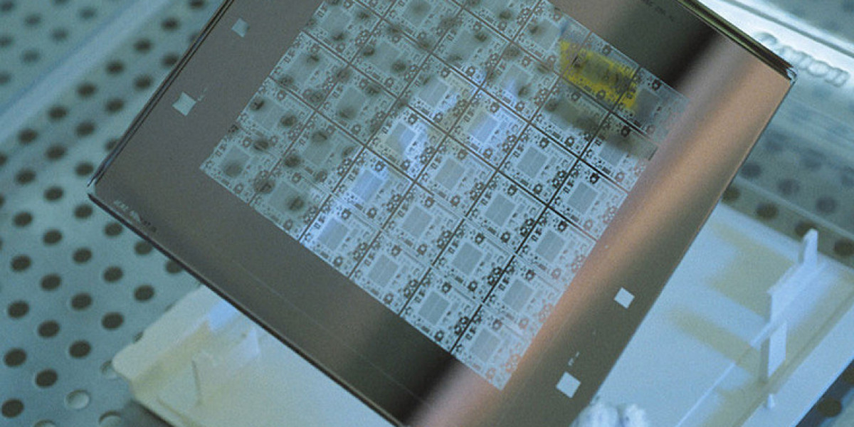
One of the most significant developments driving change in the photomask inspection landscape is the transition from traditional deep ultraviolet (DUV) lithography to extreme ultraviolet (EUV) lithography. EUV is essential for manufacturing advanced nodes at 7nm and below, but it brings new challenges to mask creation and inspection.
Traditional inspection tools are not sufficient for detecting the new types of defects introduced by EUV. This has led to increased demand for:
Actinic inspection systems, which operate at the same 13.5 nm wavelength as EUV light
Multilayer inspection capabilities to handle complex mask structures
Higher-resolution inspection for sub-nanometer accuracy
This technological shift is prompting fabs to invest in more advanced tools and processes, signaling a long-term transformation in inspection methodologies.
Integration of Artificial Intelligence and Machine Learning
Another major shift is the integration of AI and machine learning (ML) into photomask inspection systems. With AI, manufacturers can now:
Analyze inspection data faster
Classify defects with greater accuracy
Reduce false positives
Adapt inspection parameters automatically based on real-time feedback
AI-enabled systems are also paving the way for predictive maintenance, allowing fabs to anticipate failures or inconsistencies before they occur. This significantly improves production efficiency and lowers overall costs, making AI a central feature in modern photomask inspection platforms.
Shift Toward Hybrid and In-Line Inspection Solutions
To meet the growing demand for speed and accuracy, tool developers are introducing hybrid inspection systems that combine optical, electron-beam (e-beam), and actinic technologies. These multi-modal systems are designed to:
Address a broader range of defect types
Provide faster throughput
Maintain high-resolution detection capabilities
Furthermore, there is a growing trend toward in-line inspection, where systems are integrated directly into the production flow. This allows real-time detection and classification, helping manufacturers correct errors on the fly and improve overall yield.
Market Shifts Driven by Geopolitics and Localization
Recent global disruptions have emphasized the importance of supply chain resilience and regional independence in the semiconductor industry. This geopolitical shift is influencing the photomask inspection market in several ways:
Countries like the U.S., China, and members of the EU are heavily investing in domestic semiconductor production
Demand for localized photomask inspection tools and services is rising
Governments are offering incentives for semiconductor and inspection tool manufacturers to build local capacity
These changes are expanding the photomask inspection market beyond traditional hubs like Taiwan and South Korea, opening new opportunities in emerging regions.
Increasing Demand for High-Performance Chips
The demand for advanced applicationssuch as artificial intelligence, autonomous vehicles, and IoTis accelerating the need for high-performance, low-power chips. These chips often require complex mask patterns with nanometer-scale features, increasing the potential for photomask defects and driving the need for robust inspection systems.
As a result, semiconductor manufacturers are:
Upgrading older fabs with new inspection tools
Increasing inspection frequency throughout the mask lifecycle
Partnering with specialized tool providers for advanced solutions
This shift reflects a deeper integration of inspection systems into the overall chip design and fabrication ecosystem.
Future-Proofing Through RD and Collaboration
With the photomask inspection market in flux, collaboration and innovation are becoming essential. Leading companies like KLA, Lasertec, and Applied Materials are investing in research and development to stay ahead of emerging defect types and design complexities.
Key areas of focus include:
Development of AI-driven inspection algorithms
Compact, high-speed tools for smaller fabs
Collaborative platforms for data sharing and cloud-based inspection analytics
These initiatives are helping the industry prepare for the next wave of photomask complexity and ensuring that inspection tools evolve in lockstep with lithography and design trends.
Conclusion
The photomask inspection market is undergoing significant shifts as it adapts to the demands of modern semiconductor manufacturing. From the rise of EUV and AI integration to geopolitical pressures and evolving chip architectures, the landscape is more dynamic than ever.
For industry players, keeping pace with these shifts means embracing innovation, investing in scalable tools, and collaborating across the semiconductor value chain. As photomask inspection becomes a cornerstone of high-yield manufacturing, its role will only grow in importancemarking it as a key enabler of the digital future.
Learn more: https://www.pristinemarketinsights.com/photomask-inspection-market-report